Assignment:
A- Group exercise
B_ Make the board/FabISP in-circuit programmer.
C_Stuff the board-components + soldering.
D_Program the board.
C_Stuff the board-components + soldering.
D_Program the board.
A- Group exercise
I had already documented this assignment in previous year when there were no group assignment. Consequently the information of the group assignment may be redundant with some information of my formal documentation. While in previous and next weeks I may be doing the group assignment individually this time I did it with 3 classmates.
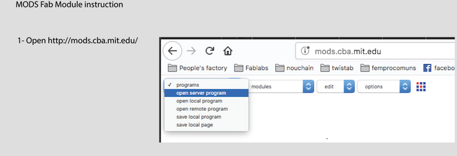
I got used to Fab Modules in the last years and really enjoyed working with it. This year Neil has released the modern version called MODS. It is a more developped version with interactiv functionality. The interface is designed as nodes that can be configured and connected together to generate and/or prepare file for digital fabrication. It integrates protocols, setting and parameters for all (and more) machines of the fablab inventory.
B_Make the FabIsp in-circuit programmer.
A FabISP is an in-system programmer for AVR microcontrollers, and it is used to load program onto the microcontroller. First we need to phisically produce the board, then stuff it with components and finally load it with a program. Once loaded it will acquire the capacity to be used to program other Isp board.
The Usbtiny44 we are making is designed to be made in Fablabs.
I found helpful to review the different versions that are proposed in the class archive to get a better understanding of what is a FabIsp, its function and get familiar with the basic electronic components.
Building the FabTinyISP
FabISP, a fab-able in-system programmer
FabTinyStar
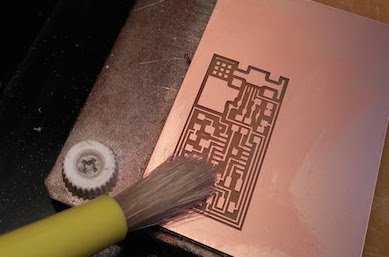
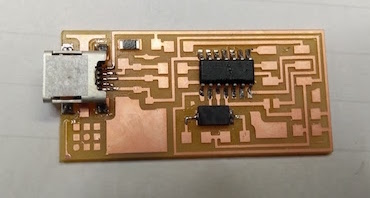
Milling the board consists of removing specific areas of the boards copper layer using a desktop CNC mill. Our lab is equiped with a Roland Modela SRM20 and that is the machine I will be using.
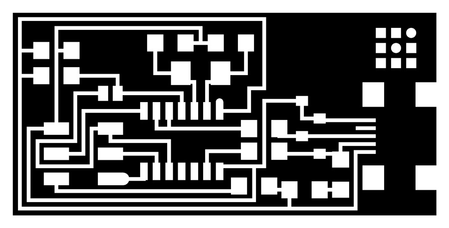
To proceed with the exercise I refered Electronic production tutorial on our lab page. I downloaded the 4 files provided in the link. The first one is an example of the finished board. The next one is the labeled board which serves as reference for tracing and to know which are the components and where they have to be placed on the board.
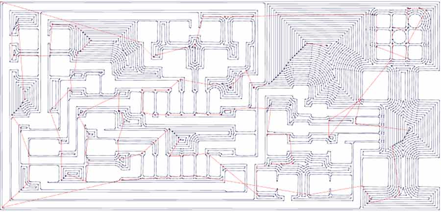
The other 2 are the files needed to mill the FabIsp. The circuit board and the board outline. Both of these files are the actual files to be milled. NOte that the part that will be milled out is the black part and only the white will remain.

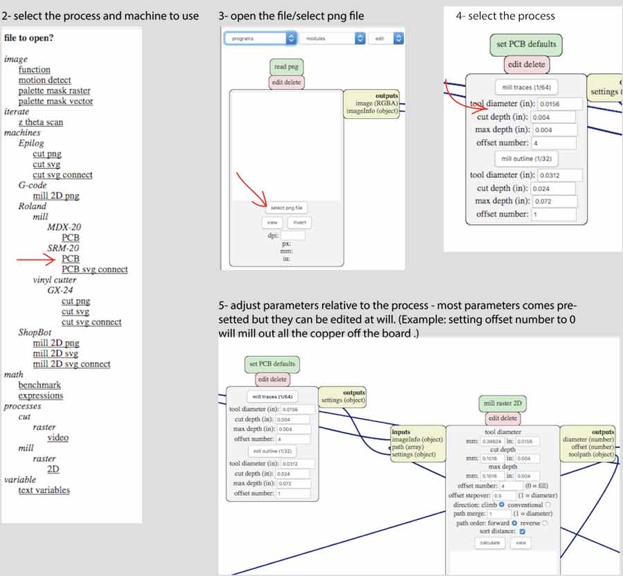
Preparing the milling files
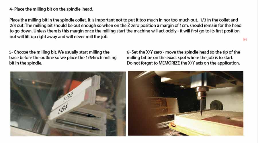
The files shown above needs to be prepared for the CNC mill to proceed. It is recommended to start milling the trace file first and the outline afterwars because if something goes wrong with milling the traces (which is THE important part) it will have to be redone and worthless having milled the outline. The TRACE file has to be milled with the 1/64 inch milling bit and the OUTLINE file has to be milled with the 1/32 inch milling bit.
I used the fab module to prepare my file. It is an application available online, it is open and integrates all the presets of the Fablab ecosystem (it has been developped for this very purpose indeed). The interface is raw but powerful, straignforward and works very well. In the main Fab Module window:
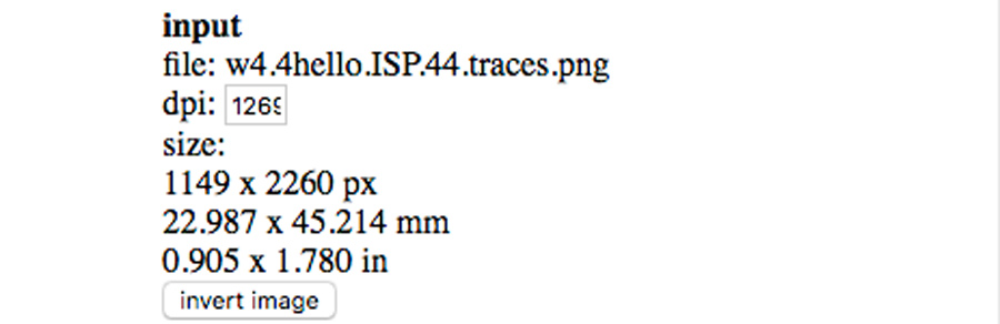
-select the input format that correspond to the file to be milled. In this case "it is" .png"
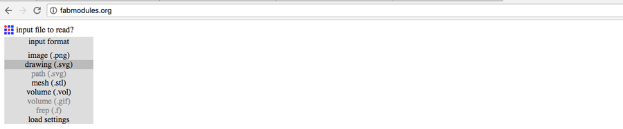
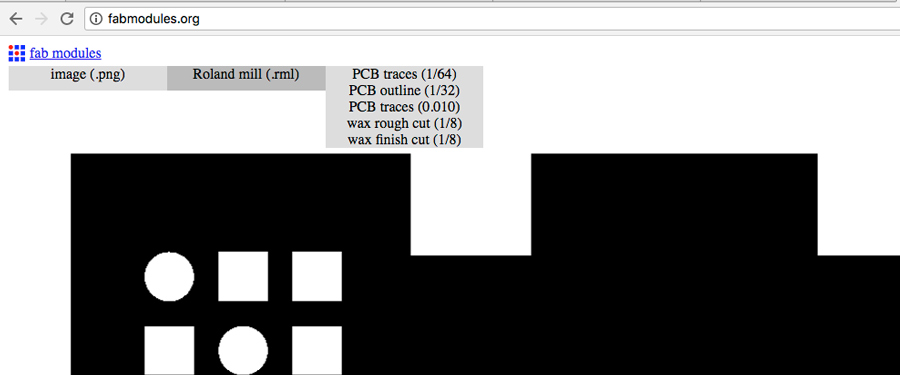
-select the file hello.ISP.44.traces.png from the desktop folder ( or anywhere it has been stored). The file uploads in the fab module window. The file opens in the fab module window. - select the Roland Mill (.rml) from the OUTPUT FORMAT tab.
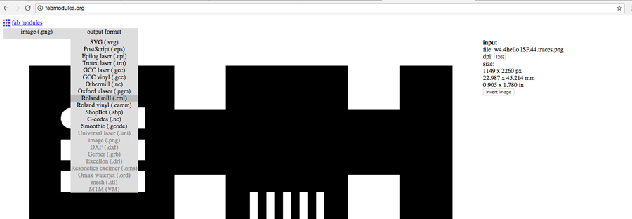
-select PCB traces (1/64).
A new window opens with a series of preset parameters corresponding to the extension of the file, the Roland desktop mill and the 1/64 milling bit. But some of them has to be edited.
-In the intput section make shure the resolution (dpi) and image size matches the file you uploaded - a difference may have a scale effect making the board useless as the trace would not fit the component path. If it is the case go back to the export file and adjust it. The FabISP should be 22.987 x 45.214 mm in size.
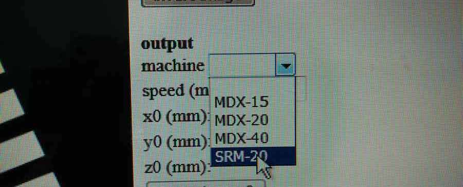
In the output section select machine: SRM20
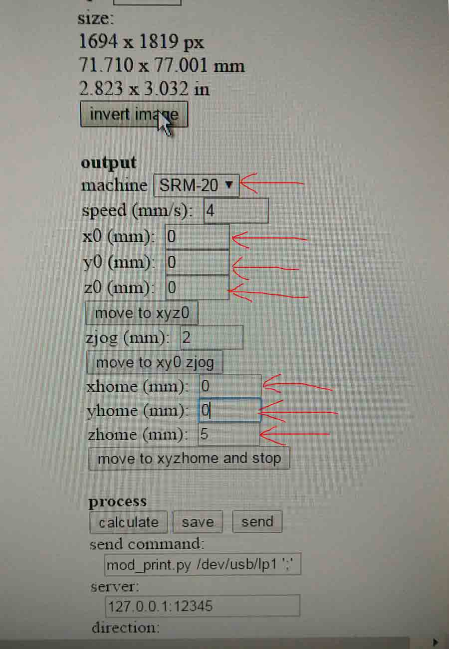
Then Fill in the other parameters as in the below pictures:
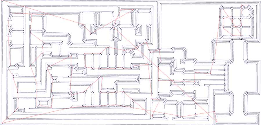
Than press calculate and the module will calculate and show the path that will be milled. It sohould look like that.
Note that not all the copper will be removed but only a section around the traces whichis fine. To leave on the copper on the trace the overlap preset needs to be set to: -1. And consequently it will slow the job as a lot more milling will have to be done. In this case the file would look like that:
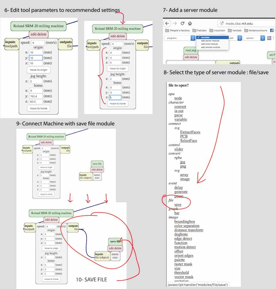
The last thing to do is to save the file (botton next to calculate botton). The file will be save in .rml format which is the format for the Roland desktop mill.
Milling
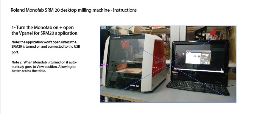
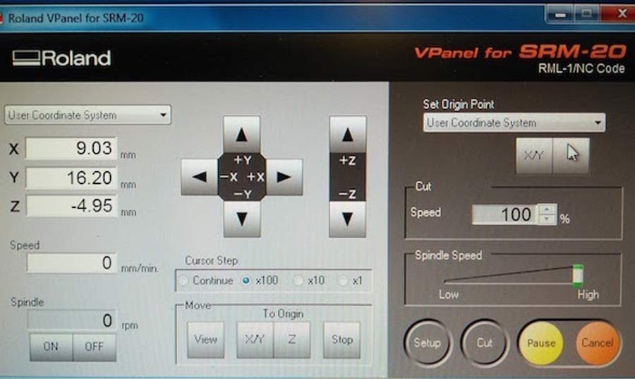
The Roland SRM 20 is user-friendly. It has its proper interface and the drivers were already installed on the lab computer that runs it.
-Make shure the usb cable is connected to the computer and turn the machine on. The machine automatically bring the table to the view position making it easier to insert the milling bit on the spindle and the board to the machine table.
-Open the Roland SRM 20 application. Once opened it will recognize that the machine is connected and is now linked. If it gives a message warning there is no machine connected it might be the cable on either hand that is not well connected.
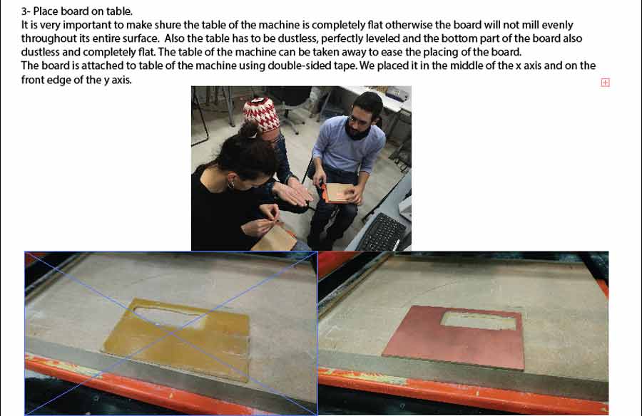
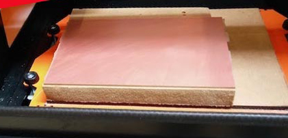
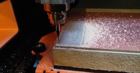
Milling is a very precise operation as we are talking about traces that are very tiny on the range of 1/64th of an inch giving little tolerance for mistakes. Preparation is an important part of the work. The first thing to do is to make shure the board is 100% flat. An easy way to do that is to lay the board at a 90º angle against a metal ruler (or any 100% flat surface) and look at it sideways against a light source. If the light spills between the board and the ruler that means it is bent and will not lay flat on the bed, and consequently the 0 of the Z axis will not be accurate throughout the whole surface of the board and therefore it might not mill completely through the copper layer making the board uselss. If it is the case either get another board or straignten it until it is completely flat.
The board will be attached to the mill table using thin double-sided tape. The surfaces of both the machine table and the board ( the white side of the board - not the copper side) needs to be cleaned very well so there are no dust remaining on either surfaces and the tape should be applied equally throuhout the whole surface of the board making shure it lays completely flat and is well attached to the machine bed. It is common in labs with many people using the Modela that the bed is not perfectly calibrated. The previous user should have notice and warn the fab manager but it is often not the case.
The usual area to place the board is on the front left corner of the table and perpendicular to the Y axis.
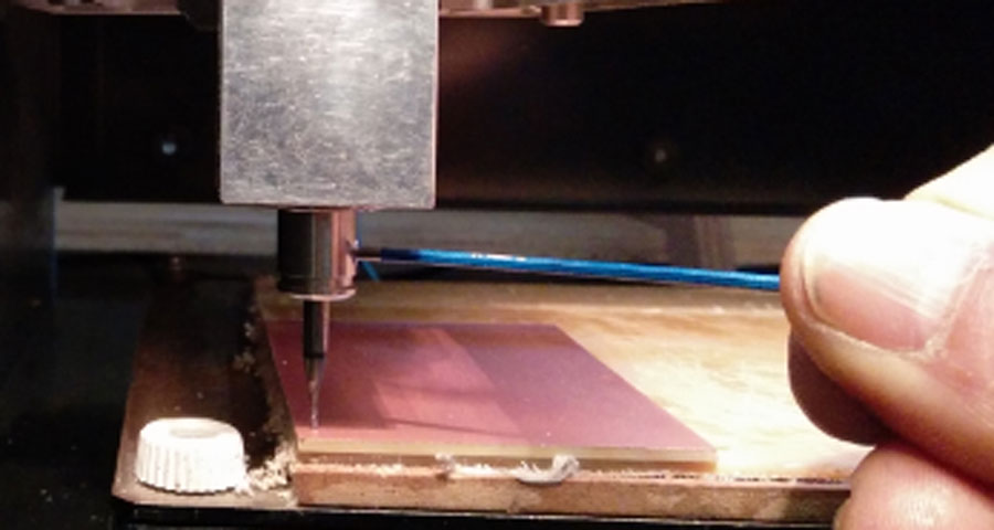
Next thing to do is to place the 1/64 inch endmill bit on the spindle, tight it with the provided Allen key - no need to tight it too strongly - It is a common mistake and it is really not necessary.
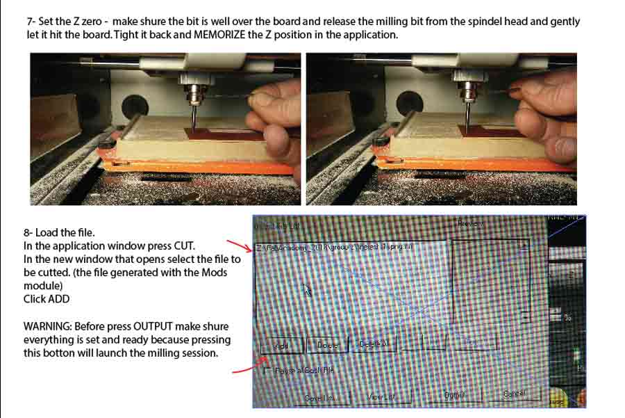
After the 0 has to be set on the Z, X and Y axis. That consists of physically placing the tip of the end mill at the exact spot where the job should start.
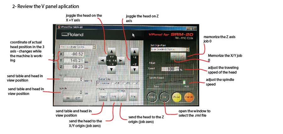
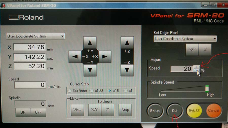
The spindle postion is moved by clicking the arrows in the SRM20 application window. There is a 4 arrows for X (left and right) and Y (backward and forward). I first set the XY by moving the spindle to the corner (front left) of the board leaving a little margin of 2 mm. approx. Than pressed the XY botton in the "set origin point" section of the appication.
Move the spindle a little bit away from the edges of the board and carefully lower it down until it is about 50 mm above the board. Then loosened up the endmill and let it fall until it touches the board. Tighten the endmill back to the spindle.
DO NOT FORGET to press the Z botton below the "set origin point" of the application window. Now the X,Y and Z are set and ready to mill the job. It is important to remember that the X and Y zeros should never be changed while milling one job.
In the application window press CUT. That opens a window asking to select a file.
-Deselect all the file from that window.
-Select the trace file (with the .srm extension) created from the Fab Module.
- Press ADD
- Press OUTPUT -
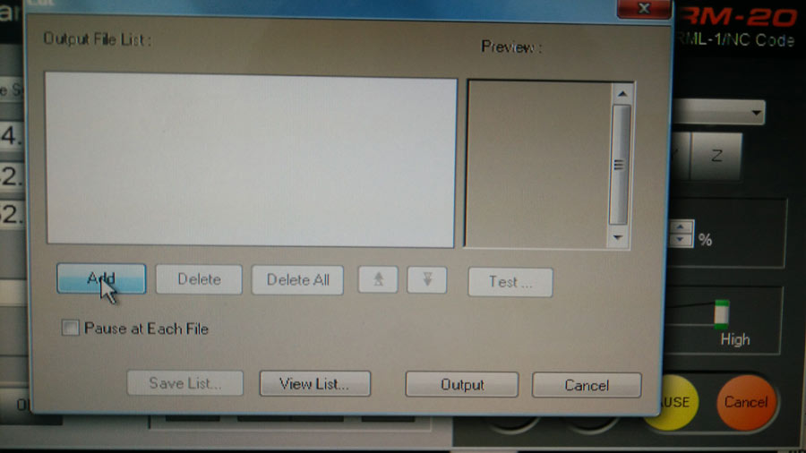
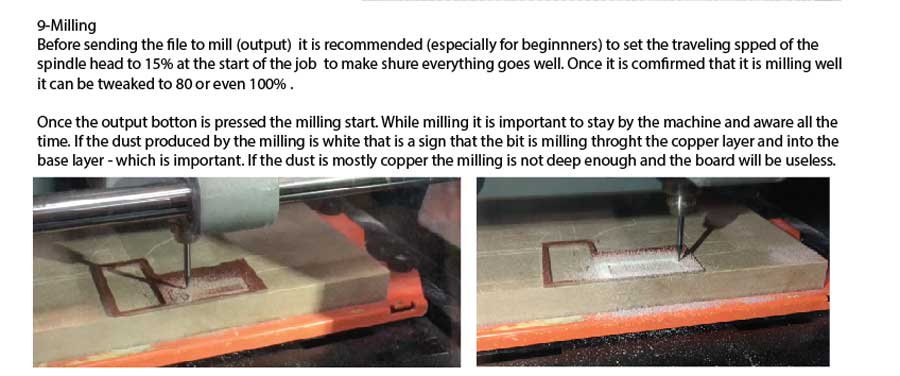
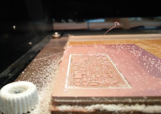
Milling will start.
NOTE: It is convenient to ADJUST the speed to 20% at the beginning of the job to make shure it is all ok. It can be brought to 100% than without interupting the job.

The dust created by the end mill should be whitish all through the path indicating it is milling through the copper layer. If not it means the board or the table is not flat and the board won't be usable. To remedy that the job can be resend after adjusting the Z axis a 1/1oth of mm. down. If so make shure the board has not been moved.
It was the first board I was millling and I spent the all time watching it as if I was watching TV.
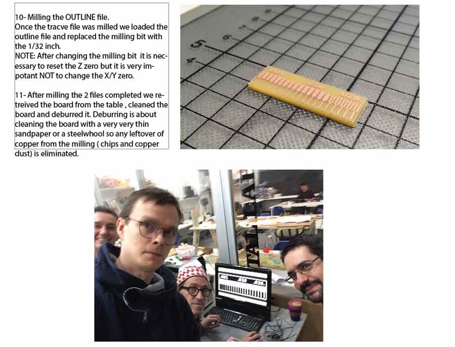
Once the tracing completed, I replaced the endmill with the 1/32 inch, reset the Z axis (not forget to comfirm the Z origin in the application window) and loaded the outline file on the fab module, set the job to PCB outline(1/32) end mill.
During this operation it is crucial not to change the Xand Y setting It is important not to move the board from the bed and not to loose the O on the X/Y axis.
Once milling completed the board has to be deburred:
-scratch out the chips of metal on the trace edges gently with a fine sand paper or a rigid flat surface.
- clean the copper face of the board with alcohol to retrieve traces of grease.
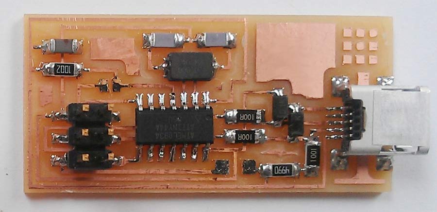
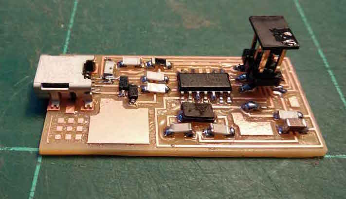
B_Stuffing the board
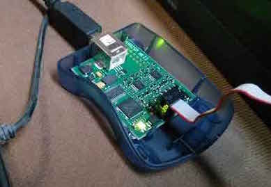
Stuffing the board consists of soldering the components onto the board in their right position and orientation. I selected each components and stuck them to a a sheet of paper where I have listed them. Components are small and can be easily mismatched.
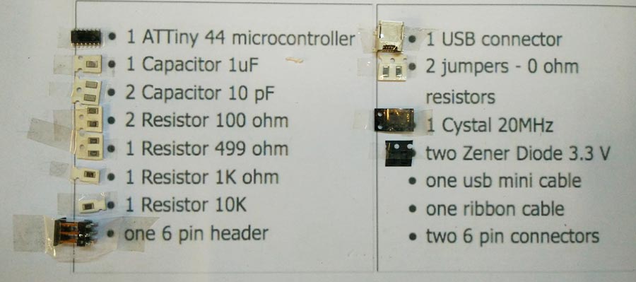
Notes on components
- The order of the description corresponds to the order the components were soldered on the board.
- The Mini Usb Connector -J2USB- will connect the FabIsp to the programmer. It is recommended to solder it first onto the board since it is the more difficult and risky.
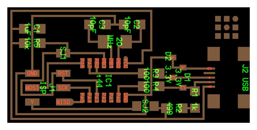
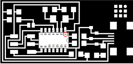
- The Microcontroller "IC1 t44" in the diagram is an attiny44 chip. There is a little circle on the top left of the component when oriented in the same direction of the diagram.
- Crystals do not have polarity, orientation do not matter.
- Diodes have polarity. The "C" or cathode end is marked with a tiny line. Important to place the side with the line over the "C" side pad in the diagram.REMEMBER CURRENT ALWAYS TRAVEL FROM A (+ anode) to C (- cathode).
- Resistors are marked with an "R" (R1, R2, etc).Resistors do not have polarity, orientation does not matter. But they have a value and diferent resistors are used for different purposes. The value of a resistors is written on the resistor through color stripes. See
code for resistors numberingchart.
- Capacitators are marked with a "C" (C1, C2, etc) Capacitors do not have polarity, orientation does not matter.
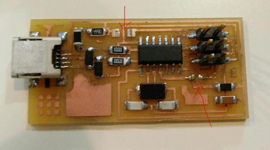
- The components marked SJ1 and SJ2 are solder jumpers. No polarity. Those will be removed once the board has been programmed.
- The components marked J1 ISP is the 6 pin programming header.Orientation does not matter.
Soldering the components to the board was a challenge as it is the first time I was dealing with such small components but alltogether it went well.
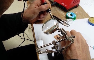
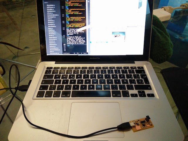
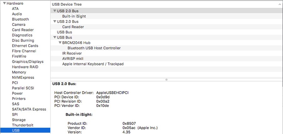
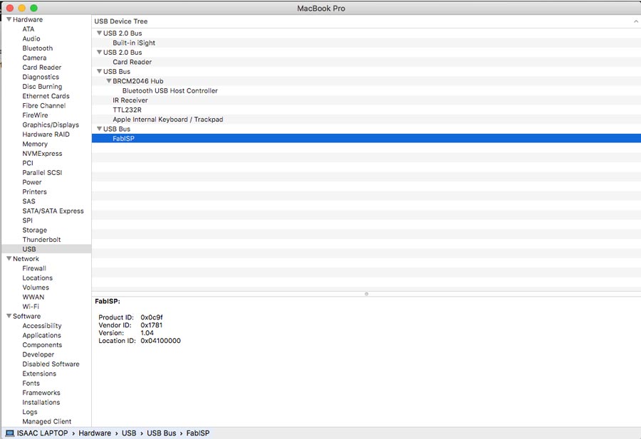
Once the stuffing was done I crossed my finger and connected the Fab Isp to the USB port of my computer and get a positive response. To verify the FabISP is connected and recognized by the system in MacOS go to : "about this mac" and open the system report window and click the USB device list. An "AVRISP" (until the board is programm it is not yet a programmer and shows listed as AVR ISP) shows in the list.
C_Programming the FabIsp
Now that I comfirmed the board mounts it need to be programmed. The programming consist of embedding the microcontroller with the capacity to become a programmer. For this to happen a program needs to be uploaded onto the FabISP using a programmer which can either be an AVRDUDE external programmer or another FabISP that has alkready been programmed. The advantage of the AVRdude is that it has a led signal that help identifying connection and troubleshoot. The programmer needs to be connected to the computer and its 6 pin connector to the 6 pin header of the FabIsp. Very important to make sure OF MATCHING THE POLARITY OF THE AVR PROGRAMMER NEGATIVE PIN WITH THE NEGATIVE PIN OF THE FABISP. OTHERWISE THAT CAN CREATE A SHORT CIRCUIT AND SCREW THE BOARD. When properly connected a green light will turn on the AVR programmer and the code can be loaded into the microcontroller).
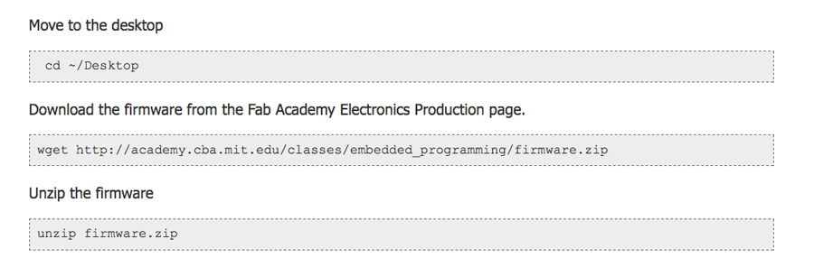
The code files required to program the FabISP are available in the Fab Academy web page .
To program the FabISP from a MacOs Xcode and Croospack AVR need to be installed. (I already have them installed on my computer). It can be downloaded from the Apple developper and the Crosspack AVR that comes with the installer.
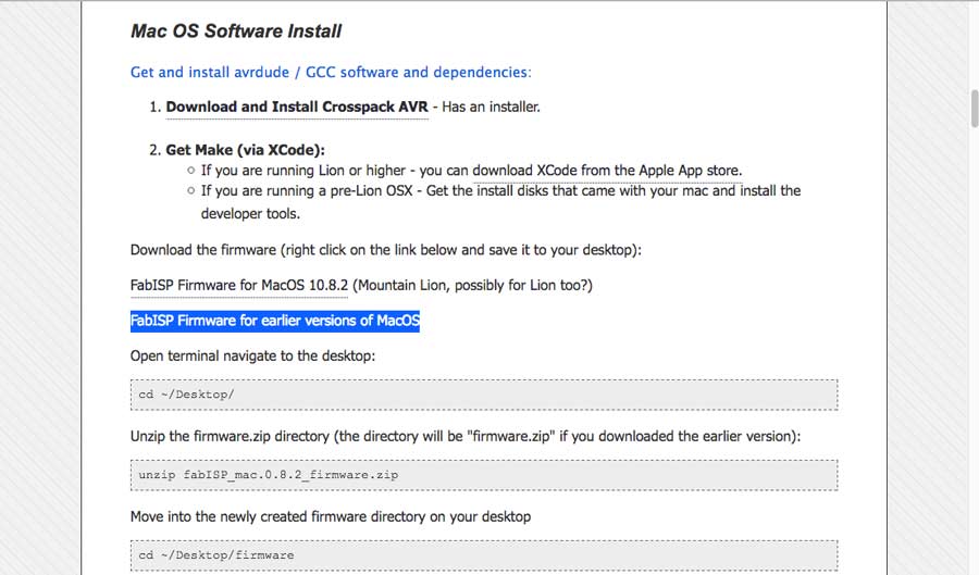
This last line of the the tutorials did not connected to the file that was unzipped. I realized it and type the correct command:
cd ~fabISP_mac.0.8.2_firmware

Once the firmware is downloaded and, in the terminal window we are in the firmware directory, we need to run the code that will program the FabISP. These code files are actually normal text files that can be edited as simple texts. In this case the code is written and only needs to be ran from the terminal.
I opend the files (from the uncompressed firmware folder.
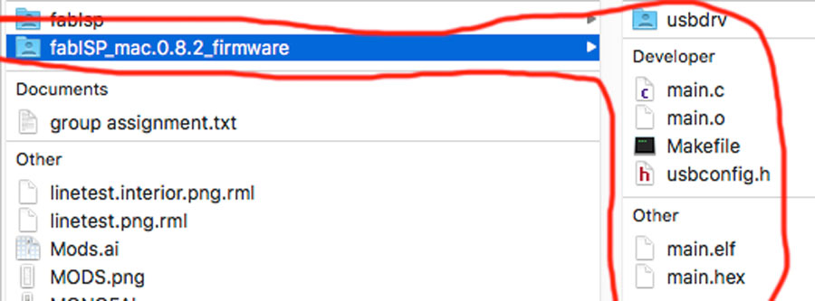
At this point there are only 4 files (makefile, main.c, usbconfig.h and the usbdrv).
Then I ran the makefile (make hex and make fuse) and got a comfirmation. Meaning the FabISP is ready to be programmed. Then I ran the program command and the code loeaded on the FabISP.
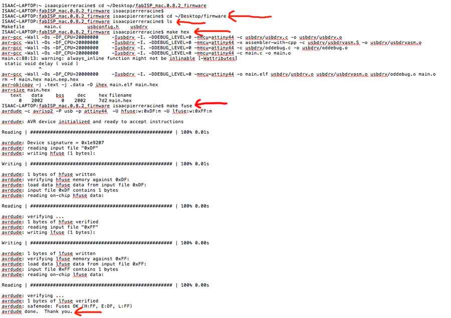
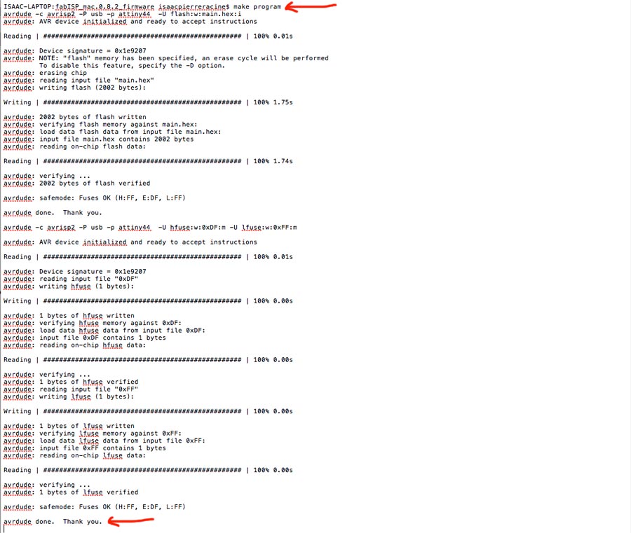
Getting the thank you message as the last code line was an amazing satisfaction. Now that the FabISP is programmed it can be used to program other board - making the same function as the AVR controller. It will be helpful in the near future to programm the boards during the next electronic assignments.
For the FabISP to be used as a programmer the 2 components we listed as "solder jumper" needs to be removed.
Undrerstanding basic electronic
As I am very new to electronics and programming as I went along with this assignment I reviewd basic electronic notion and concepts. This series of tutorials were very helpful: Demystifying the FabISP and Designing the FabOptimus

Conclusion
I felt very lost throughout the whole procees of this assignments. I honestly do not understand very well what I did and what it all means. I have researched everything I did not understand but even though it still feel very abstract. Especially when it comes down to the .kex files, make files and electronic concepts sand the function of each components. I will continue studying on my spare time and will get more familiar as time goes. As per the practicle aspect of the exercise it was easier. I made the beginners mistake such as forgetting to comfirm the o axis on the SRM application after having set the endmill on the spindle, inverting the Diodes polarity but none of that was big issue. I am very satisfied with what I managed but scared of all I have to learn.